
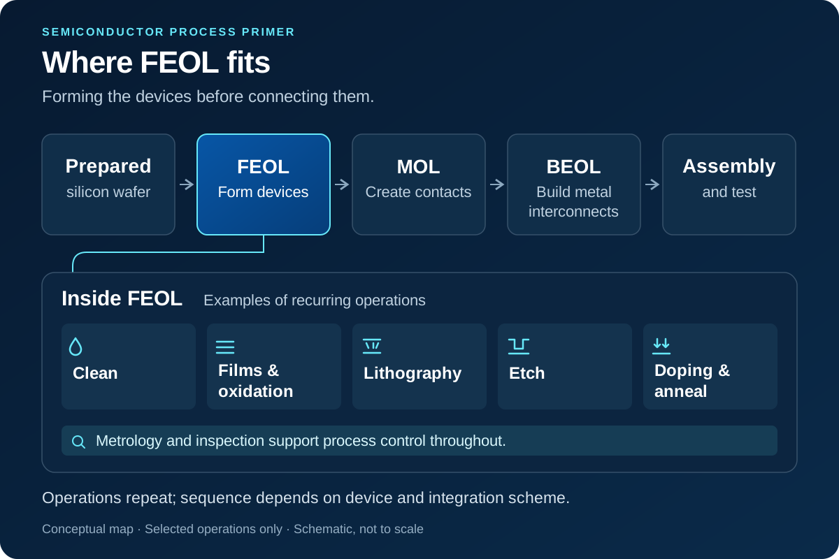
A semiconductor chip is built by repeatedly changing selected areas of a wafer. Some operations add material; others remove it, define a pattern or change electrical behavior. Understanding those jobs makes a complex fabrication flow easier to follow—and explains why the equipment surrounding the wafer matters.
First, what does “front end” mean?
Front-end manufacturing usually means wafer fabrication as a whole. Front-end-of-line (FEOL) is narrower: it forms transistors and other device elements. Middle-of-line (MOL) creates their local contacts; back-end-of-line (BEOL) builds the interconnect wiring. Assembly, packaging and final device testing are later activities. BEOL is therefore not another name for packaging. This guide focuses on FEOL while showing its place in the wider route. Lam Research: technical glossary.
The incoming wafer is already a manufactured substrate. Growing a silicon ingot, slicing it and preparing a polished wafer are upstream activities, distinct from building transistors on that wafer. SUMCO: wafer production.
A repeated set of operations, not one universal recipe
A useful way to read a fabrication flow is to ask: what must be added, patterned, removed or modified next? A device requires many such operations, with cleaning and measurement between selected steps. The order and frequency depend on the device architecture and process integration; a teaching diagram is not a production recipe. ASML: manufacturing overview.
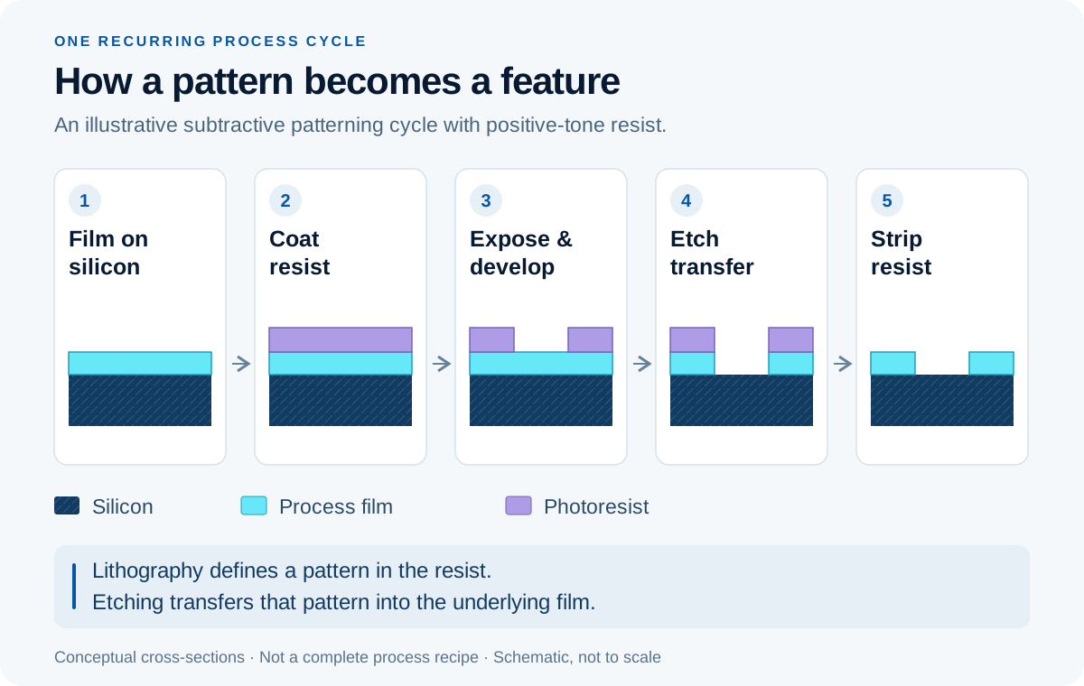
For example, a layer may be formed, covered with resist, patterned, etched and cleaned. Another region may instead receive dopants. Thermal treatment or planarization may follow where required. The wafer returns to different tools as its structures develop; it does not simply pass through each process once.
1. Clean and prepare the surface
Cleaning removes unwanted material and prepares the wafer for the next operation. Residues from one step can interfere with the next, so cleaning recurs throughout fabrication. Depending on the surface and residue, processing may use wet chemicals or dry methods. Photoresist stripping removes the temporary patterning material after it has served its purpose. The objective is controlled removal without unacceptable damage to the intended structure. Lam Research: strip and clean applications.
2. Grow or deposit the required film
Oxidation and deposition are related, but different. In thermal oxidation, silicon at the wafer surface reacts to form silicon dioxide. That oxide can provide insulation or protection. Device designs also use other dielectric materials, so “gate dielectric” does not always mean a simple thermal oxide. SK hynix: oxidation explained.
Deposition adds a chosen film to the surface. Chemical vapor deposition (CVD) and atomic layer deposition (ALD) are examples; ALD builds films through controlled reaction cycles. Insulating and conducting films serve different functions. The required material and geometry determine the process choice, rather than one method being suitable for every layer. Lam Research: deposition.
3. Define where the next change should happen
Lithography creates a temporary pattern in a light-sensitive coating called photoresist. Light exposure changes the resist chemistry; development then removes selected areas. The remaining resist defines protected regions and openings for a later operation. Lithography does not itself cut the underlying material into its final shape. ASML: photoresist and lithography.
4. Transfer the pattern by removing material
Etching removes selected material so the temporary pattern becomes a physical feature. Dry etching commonly uses plasma; wet etching uses liquid chemistry. The process must balance the shape of the feature with selectivity—the ability to remove one material while limiting removal of another. Resist or another masking layer protects regions that should remain. After pattern transfer, stripping and cleaning prepare the surface for subsequent work. Lam Research: etching.
5. Modify electrical properties and apply heat
Doping introduces selected elements into the semiconductor to change its electrical behavior. Ion implantation delivers dopants into chosen regions. Implantation can disturb the crystal lattice, and a later thermal treatment can repair damage and activate the dopants electrically. Diffusion is another important mechanism by which dopants move through the material. These operations must be coordinated with the structures already present. Applied Materials: doping, implantation and activation.
Annealing is controlled heating used to change material properties. Different applications require different time-and-temperature exposure, so a furnace treatment and a rapid thermal treatment are not interchangeable by default. Applied Materials: thermal processing.
6. Measure, inspect and prepare the next level
Metrology measures whether features meet the intended dimensions or alignment; inspection looks for defects. For example, overlay describes how accurately one patterned layer aligns with another. Measurements support process control and correction, rather than being only a final pass-or-fail test. ASML: measuring accuracy.
Where the integration requires it, chemical mechanical planarization (CMP) removes material using chemical and mechanical action to make the surface more planar. CMP, cleaning and metrology can appear at different points in fabrication; none is exclusive to FEOL. Applied Materials: technical glossary.
Where quartz equipment components fit
The finished transistor is not made from a quartz boat or process tube. These are equipment components that support or surround the wafer during selected operations. Batch thermal and deposition equipment can process wafers in horizontal or vertical tube furnaces, with carriers holding multiple wafers. Quartz material selection depends on the application. Heraeus Conamic: semiconductor quartz applications.
This creates a practical connection to several WONIK product families:
- Quartz process tubes form drawing-specific process enclosures, with ports and sealing interfaces matched to the intended equipment.
- Quartz wafer boats and vertical quartz boats support substrates; slot geometry, loading method and orientation matter.
- Quartz gas-delivery components provide application-specific gas paths, with port locations and mating interfaces defined during review.
- Quartz wet-process tanks are candidates for compatible chemistries; concentration, temperature, circulation and leak criteria must be established first.
Quartz is not universally compatible with wet processing. Hydrofluoric acid attacks fused quartz, and alkaline contamination can create problems during subsequent heating. A familiar process name is insufficient to select a tank or chamber material. Momentive Technologies: quartz usage guidelines.
For a component enquiry, share the drawing revision, process gases or liquids, temperature profile, pressure, loading arrangement and acceptance criteria. WONIK can then review the appropriate product family and manufacturing scope. These examples explain possible roles; they do not establish compatibility with every tool or recipe. Explore quartz product families or discuss your application.
References
- Lam Research — Technical Glossary: FEOL, MOL, BEOL and packaging terminology.
- SUMCO — Production Processes: preparation of silicon wafer substrates.
- ASML — Six Crucial Steps in Semiconductor Manufacturing: repeated processing and patterning principles.
- Lam Research — Reliant Clean Products, Deposition and Etch: the jobs performed by these process families.
- SK hynix — Protecting Key Components Through Oxidation: oxide formation and device insulation.
- Applied Materials — Technical Glossary and Thermal Processing: doping, activation, CMP and thermal treatment.
- ASML — Measuring Accuracy: overlay, metrology and process feedback.
- Heraeus Conamic — Clear Fused Silica for Semiconductor Manufacturing: quartz applications in semiconductor equipment.
- Momentive Technologies — Usage Guidelines: chemical exposure and contamination considerations.
The diagrams are original explanatory illustrations. They are not photographs, equipment drawings or operating instructions.